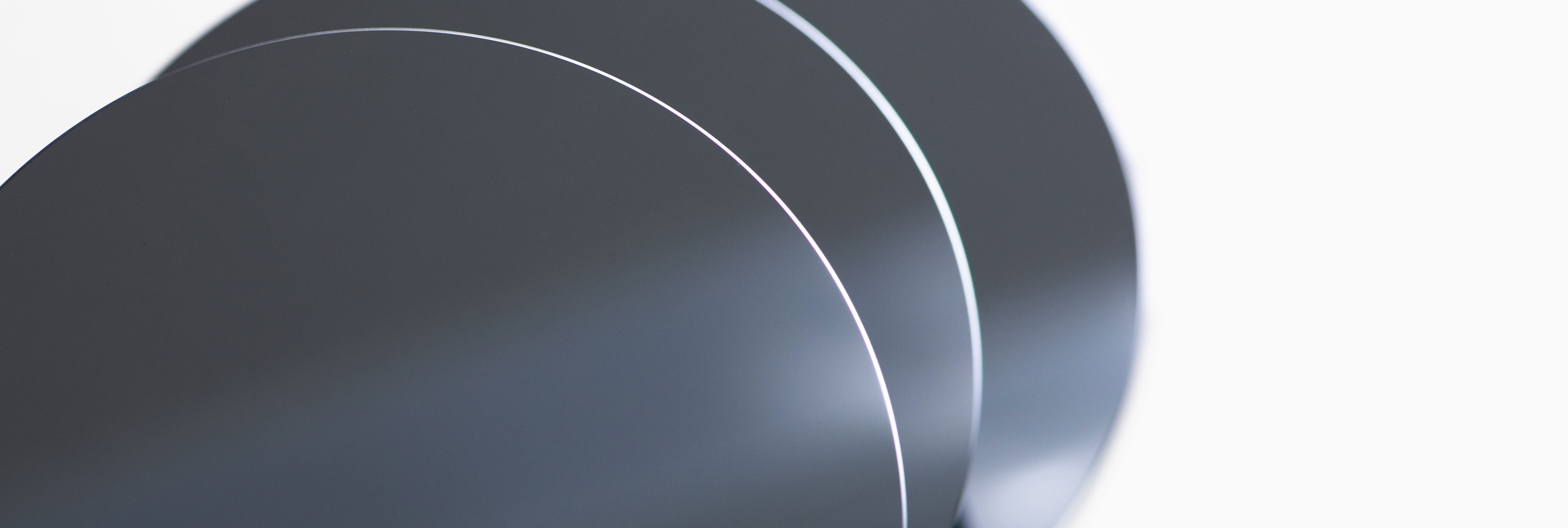
Gallium Arsenide (GaAs)
- Elements
- Gallium (Ga), Arsenic (As)
- Substance Type
- Compound Material
Elements, Chemical Composition and Structure
Gallium Arsenide (GaAs) is the first naturally nonexistent, artifically manufactured semiconductor. It has a zincblende crystal structure at room temperature and is slightly toxic. It contains arsenic, which is considered a carcinogen, and therefore requires special treatment during its disposal. Acids, steam and heat involved during its processing can contribute to the formation of arsine, therefore requires further caution. Because it has higher electron mobility than the widely used silicon, they are used as a substrate material for high speed communication applications like smartphones and other mobile devices. Because GaAs is a direct band gap semiconductor, they are also used in infrared light emitting diodes (LEDs). They are also very popular as the substrate material for vertical cavity surface emitting lasers (VCSELs), a technology that is expected to be used in facial recognition systems.
| Chemical Formula | GaAs |
|---|---|
| Crystal Structure | Zincblende |
| Melting Point | 1238℃ |
| Electron Mobility | 8,500 cm2/(Vs) |
| Band Gap | 1.43eV (300K) |
Properties
Compared to that of silicon, the most common semiconductor, gallium arsenide has 5-6 times higher electron mobility and high electrical resistivity. These properties make it very suitable for high speed process applications and therefore is known for semiconductor component with low electricity consumption.
Production
Single crystal gallium arsenide is grown using Liquid-Encapsulated Czochralski (LEC) method, similar to silicon crystal growth. It involves pulling a seed crystal rod from a crucible, however, in order to prevent arsenic from evaporating, boron trioxide is also added to the crucible. As a result of heating the crucible, Boron trioxide melts and encapsulates the melt. While LEC is suitable for growing large diameter GaAs ingots, one disadvantage is its high dislocation density. Ingots with lower dislocation density can be grown using the Horizontal Bridgman method; however, growing large diameter ingots is usually difficult with this method.
Practical Applications
Gallium Arsenide offers high-speed computing capabilities due to its superior electron mobility and it is used in high frequency wave devices like smartphones and base stations. Because it is a direct band gap semiconductor, they are also used in in infrared LEDs and semiconductor lasers.
Its demand as a VCSEL substrate material has also been increasing in the recent years.
DISCO's processing solutions
DISCO's grinders, dicing and laser saws can be used when cutting and grinding GaAs.
If you require solutions for your processing issues,
please contact DISCO CORPORATION.
-
Please contact DISCO CORPORATION.
Please feel free to contact us through the inquiry form or via phone call.
Inquiries -
Consultation for non-chargeable processing
If you are struggling with any processing issues,
please contact DISCO.Service details -
Easy confirmation in thirty seconds!
Online processing feasibility confirmationJust enter the conditions
Easy processing evaluation


